Exploring Logic Gates
The Exploring Logic Gates lab is designed for you to explore the basic logic gates, simple logic circuits and truth tables. You will be using Digital Simulator, a simulation tool for logic gates and other computer hardware.
IMPORTANT: Setup
Download and extract to a convenient place on your OneDrive or other cloud storage centre so the application is accessible on any machine you use.
Digital source code and project can be found on here:
OR ...
-
From here logic_simulator
-
Once downloaded place in your OneDrive and unzip. Navigate to the
Digitalapplication and run. -
If you're a
Linuxuser, after downloading the folder:-
Unzip it.
-
Open the terminal and navigate to the directory where you placed the simulator.
-
Run the following command:
bash Linux_Digital.sh
-
Full documentation of the simulator can be found here and here
Task-1
In this exercise you are going to familiarise your self with placing components and operating the Logic Gates.
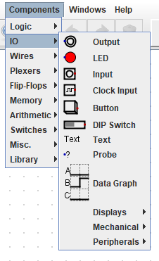
The image below shows the location of where you will find the Input and Output components. You will need to select at least one Output and one or two Input components:
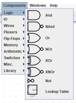
Next logic gates are selected as seen in the image below:
NOT Gate
Firstly, set up the the circuit in below:

Press the the play icon, ►, and toggle the input component labelled as 'A', does it behavior as per the truth table below?
| A | S |
|---|---|
| 0 | 1 |
| 1 | 0 |
CALL TO ACTION
Save the circuit in OneDrive call it
Logic-Gates-Exercise-1
OR Gate
Continuing in the same file add the OR gate underneath the NOT circuit so that your new circuit looks like below.
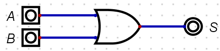
Press the the play icon, ►, and toggle the input component labelled as 'A' and 'B', does it behavior as per the truth table below?
| A | B | S |
|---|---|---|
| 0 | 0 | 0 |
| 1 | 0 | 1 |
| 0 | 1 | 1 |
| 1 | 1 | 1 |
CALL TO ACTION
Re-save the circuit again.
AND
Continuing in the same file add the AND gate underneath the OR so that your :new circuit looks like the image below.
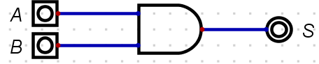
Press the the play icon, ►, and toggle the input component labelled as 'A' and 'B', does it behavior as per the table below?
| A | B | S |
|---|---|---|
| 0 | 0 | 0 |
| 1 | 0 | 0 |
| 0 | 1 | 0 |
| 1 | 1 | 1 |
CALL TO ACTION
Re-save the circuit again.
XOR
Continuing in the same file add the XOR gate underneath the AND circuit so that your new circuit looks like the image below:
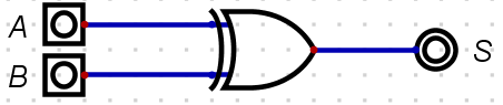
Press the the play icon, ►, and toggle the input component labelled as 'A' and 'B', does it behavior as per the truth table below:
| A | B | S |
|---|---|---|
| 0 | 0 | 0 |
| 1 | 0 | 1 |
| 0 | 1 | 1 |
| 1 | 1 | 0 |
CALL TO ACTION
Re-save the circuit again
XNOR
Continuing in the same file add the XNOR gate underneath the XOR circuit so that your new circuit looks like image below:
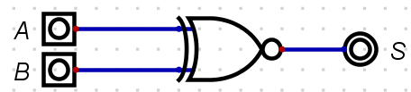
Press the the play icon, ►, and toggle the input component labelled as 'A' and 'B', does it behavior as per the truth table below:
| A | B | S |
|---|---|---|
| 0 | 0 | 1 |
| 1 | 0 | 0 |
| 0 | 1 | 0 |
| 1 | 1 | 1 |
CALL TO ACTION
Re-save the circuit again
NOR
Continuing in the same file add the NOR gate underneath the XNOR circuit so that your new circuit looks like the image below:
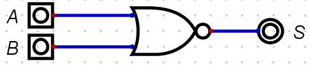
Press the the play icon, ►, and toggle the input component labelled as 'A' and 'B', does it behavior as per the truth table below?
| A | B | S |
|---|---|---|
| 0 | 0 | 1 |
| 1 | 0 | 0 |
| 0 | 1 | 0 |
| 1 | 1 | 0 |
CALL TO ACTION
Re-save the circuit again
NAND
Continuing in the same file add the NAND gate underneath the NOR circuit so that your new circuit looks like the image below:
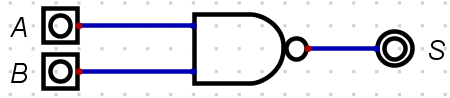
Press the the play icon, ►, and toggle the input component labelled as 'A' and 'B', does it behavior as per the truth tabel below:
| A | B | S |
|---|---|---|
| 0 | 0 | 1 |
| 1 | 0 | 1 |
| 0 | 1 | 1 |
| 1 | 1 | 0 |
CALL TO ACTION
Re-save the circuit again
Task-2: Investigation
The following universal logic gate circuits below can be constructed to create any of the fundamental gates. Investigate with the construction of truth ables match a universal logic gate circuit with a fundamental logic gate.
Universal Logic Circuit 1
CALL TO ACTION
Create a new file.
Firstly, set up the the circuit as seen below:
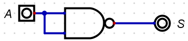
Press the the play icon, ►, and toggle the input component labelled as 'A', what fundamental gate is this?
-
AND
-
XNOR
-
NOT
-
OR
Click for solution
- NOT
CALL TO ACTION
Save the circuit in OneDrive call it
Logic-Gates-Exercise-2
Universal Logic Circuit 2
Set up the the circuit in image below and place the new circuit beneath the last circuit created.
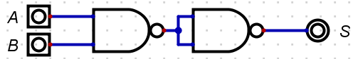
Press the the play icon, and toggle the input component labelled as 'A' and 'B', what fundamental gate is this?
-
XNOR
-
OR
-
NOT
-
NAND
-
AND
Click for solution
- AND
CALL TO ACTION
Re-save the circuit
Universal Logic Circuit 3
Set up the the circuit below and place it beneath the last circuit created.
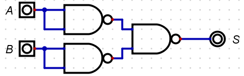
Press the the play icon, ►, and toggle the input component labelled as 'A' and 'B', what fundamental gate is this?
-
XNOR
-
OR
-
NOT
-
NAND
-
NOR
Click for solution
- OR
CALL TO ACTION
Re-save the circuit
Universal Logic Circuit 4
Set up the the circuit as seen below, beneath the last circuit created.
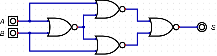
Press the the play icon , and toggle the input component labelled as 'A' and 'B', what fundamental gate is this?
Click for solution
- XNOR
CALL TO ACTION
Re-save the circuit
Universal Logic Circuit 5
Set up the circuit up as seen below, beneath the last circuit created.
Press the the play icon, ►, and toggle the input component labelled as 'A' and 'B', what fundamental gate is this?
-
NOT
-
XOR
-
OR
-
AND
-
XNOR
Click for solution
- XOR
CALL TO ACTION
- Re-save the circuit
- Go to your preferred search engine and search for 'Universal gate equivalents' and replicate the circuits we have not done in this file.
Task-3: Experimentation
You are now going to use the clock to generate signals: ON/OFF or 1/0 or HIGH/LOW or 0V/5V.
CALL TO ACTION
Create a new file.
Now get the components in the following order, so that your circuit looks like below:
-
AND Gate
-
Input
-
Clock Input
-
Output
-
Data Graph
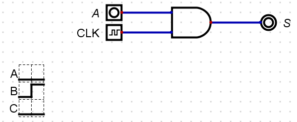
Like with all other circuits so far, right click a component and them labels as shown above.
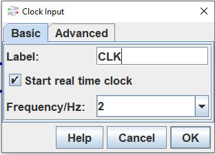
You will notice that when you right click the Clock Input you will get additional options, replicate the image below:
Make sure that the Data Graph component option Max number of steps to is set to 25.
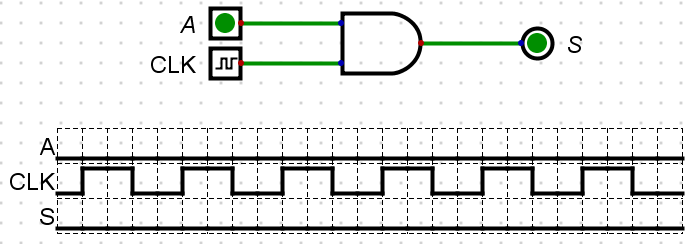
When you run this circuit you should see something similar to the image below:
CALL TO ACTION
- Save the circuit in OneDrive call it ``
- Experiment with different Clock Input Frequencies, what observations can you make? Discuss with the a peer or with the tutor.
- Replace the
with anotherand chose different frequencies. Look at the Data Graph is there a pattern? Is it random? Discuss with your peers or with the tutor.
Task-4: Investigate
You are now going to create an arithmetic circuits; Half Adder and Full Adder
CALL TO ACTION
Create a new file.
Half Adder
Reproduce the Half Adder as seen in below:
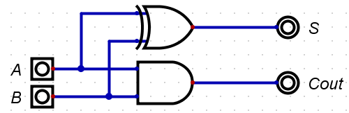 {#fig:Half_Adder}
... and then simulate so you can complete the truth table below:
| A | B | S | C_out |
|---|---|---|---|
Click for solution
| A | B | S | C_out |
|---|---|---|---|
| 0 | 0 | 0 | 0 |
| 0 | 1 | 1 | 0 |
| 1 | 0 | 1 | 0 |
| 1 | 1 | 0 | 1 |
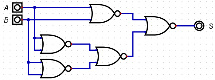
Full Adder
Produce a Full Adder and then simulate so you can populate, you should refer to the lecture slides.
| A | B | C_in | S | C_out |
|---|---|---|---|---|
Click for solution
| A | B | Cin | S | Cout |
|---|---|---|---|---|
| 0 | 0 | 0 | 0 | 0 |
| 0 | 0 | 1 | 1 | 0 |
| 0 | 1 | 0 | 1 | 0 |
| 0 | 1 | 1 | 0 | 1 |
| 1 | 0 | 0 | 1 | 0 |
| 1 | 0 | 1 | 0 | 1 |
| 1 | 1 | 0 | 0 | 1 |
| 1 | 1 | 1 | 1 | 1 |
CALL TO ACTION
- Save the circuit in OneDrive call it ``
- Experiment with different Clock Input Frequencies, what observations can you make? Discuss with the a peer or with the tutor.
- Replace the
with anotherand chose different frequencies. Look at the Data Graph is there a pattern? Is it random? Discuss with your peers or with the tutor.
Task-5: Research and Implement
Investigate & research the circuit of a 2-bit decoder, implement this and verify operation through a complete truth table and simulation.
CALL TO ACTION
Create a new file.